Category Archives: Nanowires

Silicon nanowires upgrade data-storage technology

Scientists at the National Institute of Standards and Technology (NIST), along with colleagues at George Mason University and Kwangwoon University in Korea, have fabricated a memory device that combines silicon nanowires with a more traditional type of data-storage. Their hybrid structure may be more reliable than other nanowire-based memory devices recently built and more easily integrated into commercial applications.

Continue reading

Transparent transistors to bring future displays, ‘e-paper’

Researchers have used nanotechnology to create transparent transistors and circuits, a step that promises a broad range of applications, from e-paper and flexible color screens for consumer electronics to “smart cards” and “heads-up” displays in auto windshields.

The transistors are made of single “nanowires,” or tiny cylindrical structures that were assembled on glass or thin films of flexible plastic.

Continue reading

Practical Nanowire Devices

Researchers at Harvard University and the University of Hawaii have developed an easy way to align nanowires and carbon nanotubes over areas 100 times larger than is possible using existing methods. The researchers are also able to fabricate the nanowires on a number of different surfaces. The advance potentially paves the way to mass production of electronics devices based on these promising nanostructures.

The technique, based on high-volume manufacturing methods used to produce plastic bags, could make it practical to employ nanowires and carbon nanotubes for controlling pixels on large, flexible displays and for accurately detecting multiple chemicals, viruses, and biomarkers for diseases. The results were published online this week in the journal Nature Nanotechnology.

Read rest of the story at Technology Review site.

Placing single nanowires: NIST makes the connection

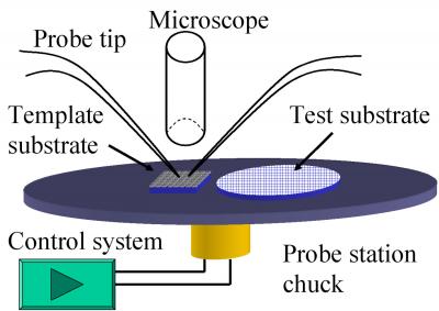
Researchers at the National Institute of Standards and Technology (NIST) have devised a system for manipulating and precisely positioning individual nanowires on semiconductor wafers. Their technique, described in a recent paper,* allows them to fabricate sophisticated test structures to explore the properties of nanowires, using only optical microscopy and conventional photolithographic processing in lieu of advanced (and expensive) tools such as focused ion or electron beams.

3875_web.jpg
Continue reading